DFT Modes
As the technology nodes are shrinking consistently, the probability of the occurrence of faults is also increasing which makes DFT an indispensable function for modern sub-micron SoCs.
What are the possible faults within an SoC and what all ways are possible to detect them? Lets discuss about this now.
Types of fault and their detection:
Structural Fault: Refers to the faults due to faulty manufacturing at the fabs. Even a tiny dust particle has cause shorts or opens in SoC.
Structural testing is done during the DFT tests or modes called as shift and stuck-at-capture. These tests are conducted after manufacturing, before shipping the part to the customer.
The scan chains are used by external automatic test equipment (ATE) to deliver test pattern data from its memory into the device. After the test pattern is loaded, the design is placed back into functional mode and the test response is captured in one or more clock cycles. The design is again put in test mode and the captured test response is shifted out, while the next test pattern is simultaneously shifted in to the scan cells. The ATE then compares the captured test response with the expected response data stored in its memory. Any mismatches are likely defects and are logged for further evaluation.
Stuck-At Test The most basic and common is the “stuck-at” fault model, which checks each node location in the design for either stuck-at-1 or stuck-at-0 logic behavior. For example, if a NAND gate in the design had an input pin shorted to ground (logic value 0) by a defect, the stuck-at-0 test for that node would catch it. The stuck-at model can also detect other defect types like bridges between two nets or nodes. The stuck-at model is classified as a static model because it is a slow speed test and is not dependent on gate timing (rise and fall times and propagation delay).
At-Speed Test A second common type of fault model is called the “transition” or “at-speed” fault model, and is a dynamic fault model, i.e., it detects problems with timing. It is similar to the stuck-at model in that there are two faults for every node location in the design, classified as slow-to-rise and slow-to-fall faults. The transition fault model uses a test pattern that creates a transition stimulus to change the logic value from either 0-to-1 or from 1-to-0. The time allowed for the transition is specified, so if the transition doesn’t happen, or happens outside the allotted time, a timing defect is presumed.
Transition Faults: Signal transitions are nothing but the voltage levels while they switch from either ‘high’ to ‘low’ or vice-versa. There is a designated time before the clock edge when all the signals should be stable at the input of the flop and also designated time after the clock edge when none of the signals should change their state at the inout of the flop. Any such fault in transition times is referred to as transition fault.
First we filter out the chips which had structural fault. Now we would test the remaining chips for transition faults. The AT-speed test is used to screen the chip for transition faults.
From another article
In this post, we would discuss the method to detect faults like- shorts and opens. i.e structural faults
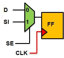
Figure shows the structure of a Scan Flip-Flop. A multiplexer is added at the input of the flip-flop with one input of the multiplexer acting as the functional input D, while other being Scan-In (SI). The selection between D and SI is governed by the Scan Enable (SE) signal.
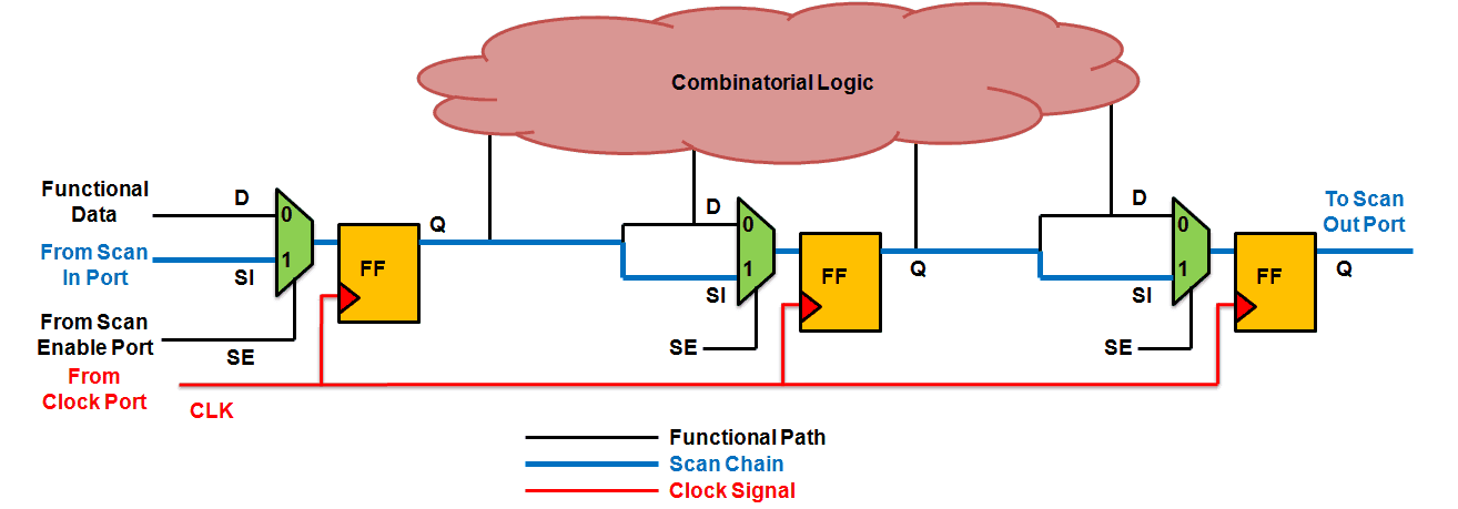
Using this basic Scan Flip-Flop as the building block, all the flops are connected in form of a chain, which effectively acts as a shift register. The first flop of the scan chain is connected to the scan-in port and the last flop is connected to the scan-out port. The Figure 2 depicts one such scan chain where clock signal is depicted in red, scan chain in blue and the functional path in black. Scan testing is done in order to detect any manufacturing fault in the combinatorial logic block. In order to do so, the ATPG tool try to excite each and every node within the combinatorial logic block by applying input vectors at the flops of the scan chain.
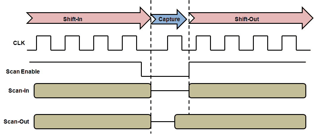
Scan chain operation involves three stages: Scan-in, Scan-capture and Scan-out. Scan-in involves shifting in and loading all the flip-flops with an input vector. During scan-in, the data flows from the output of one flop to the scan-input of the next flop not unlike a shift register. Once the sequence is loaded, one clock pulse (also called the capture pulse) is allowed to excite the combinatorial logic block and the output is captured at the second flop. The data is then shifted out and the signature is compared with the expected signature. Modern ATPG tools can use the captured sequence as the next input vector for the next shift-in cycle. Moreover, in case of any mismatch, they can point the nodes where one can possibly find any manufacturing fault. Figure 3 shows the sequence of events that take place during scan-shifting and scan-capture.
Shift Frequency: A trade-off between Test Cost and Power Dissipation
It must be noted that the number of shift-in and shift-out cycles is equal to the number of flip-flops that are part of the scan chain. For a scan chain with, let’s say, 100 flops, one would require 100 shift-in cycles, 1 capture cycle and 100 shift-out cycles. The total testing time is therefore mainly dependent on the shift frequency because there is only capture cycle. Tester time is a significant parameter in determining the cost of a semiconductor chip and cost of testing a chip may be as high as 50% of the total cost of the chip. From timing point of view, higher shift frequency should not be an issue because the shift path essentially comprises of direct connection from the output of the preceding flop to the scan-input of the succeeding flop and therefore setup timing check would always be relaxed. Despite the fact that higher shift frequency would mean lower tester time and hence lower cost, the shift frequency is typically low (of the order of 10s of MHz). The reason for shifting at slow frequency lies in dynamic power dissipation.
It must be noted that during shift mode, there is toggling at the output of all flops which are part of the scan chain, and also within the combinatorial logic block, although it is not being captured. This results in toggling which could perhaps be more than that of the functional mode. Higher shift frequency could lead to two scenarios:
Votage drop:
Higher rate of toggling within the chip would result in drawing more current from the voltage supply. And hence there would be a voltage droop because of the IR drop. This IR drop could well drop the voltage below the safe margin and the devices might fail to operate properly.
Increased Die Temperature:
High switching activity might create local hot-spots within the die and thereby increase the temperature above the worst-case temperature for which timing was closed. This could again result in failure of operation, or in the worst case, it might cause thermal damage to the chip.
Therefore, there exists a trade-off. It is desired to run the scan shift at a lower frequency which must be dictated by the maximum permissible power dissipation within the chip. At the same time, the shift-frequency should not be too low, otherwise, it would risk increasing the tester time and hence the cost of the chip!