Clock gating checks
Clock gating check is a constraint, either applied or inferred automatically by tool, that ensures that the clock will propagate without any glitch through the gate.
AND type clock gating check and OR type clock gating check.
Setup Check: This check is performed with respect to the edge of the clock that transforms the state of the clock signal from controlling state to non-controlling state.
Hold Check: This check is performed with respect to the edge of the clock that transforms the state of the clock signal from non-controlling to controlling state.
AND type clock gating check

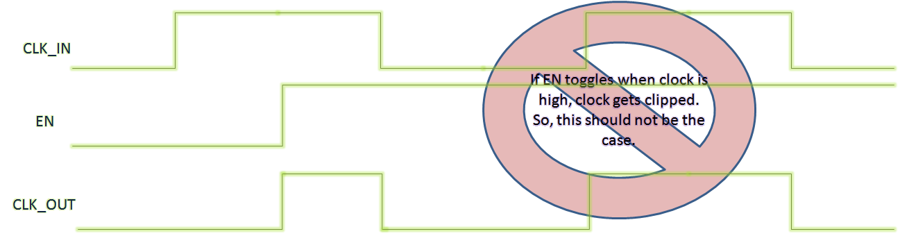
Enable shld toggle only while clock is low in case of AND clock gate.

As shown, setup check in this case is on the next positive edge and hold check is on next negative edge. However, the ratio of maximum and minimum delays of cells in extreme operating conditions may be as high as 3. So, architecturally, this situation is not possible to guarantee the clock to pass under all conditions.
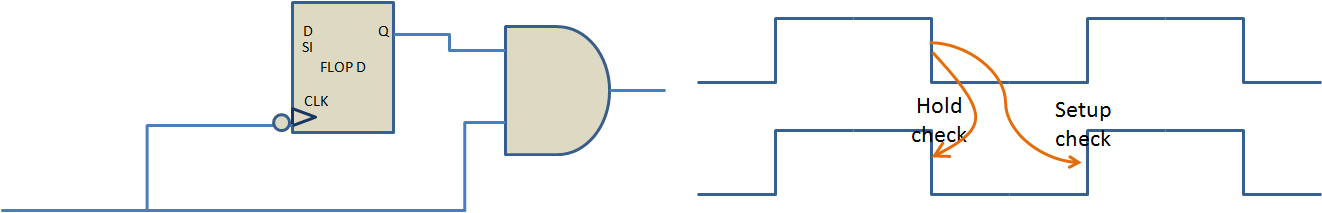
n the contrary, if ‘EN’ launches from a negative edge-triggered flip-flop, setup check are formed with respect to the next rising edge and hold check is on the same falling edge (zero-cycle) as that of the launch edge. The same is shown in figure 6. Since, in this case, hold check is 0 cycle, both the checks are possible to be met for all operating conditions; hence, this solution will guarantee the clock to pass under all operating condition provided the setup check is met for worst case condition. The inactive clock state, as evident, in this case, is ‘0’.
OR type clock gating check


In case ‘EN’ launches from negative edge-triggered flop, the setup and hold checks will be as shown in the figure 10. The setup check is on the next negative edge and hold check is on the next positive edge. As discussed earlier, it cannot guarantee the glitch less propagation of clock.

Since, the hold check is 0 cycle, both setup and hold checks are guaranteed to be met under all operating conditions provided the path has been optimized to meet setup check for worst case condition. The inactive clock state, evidently, in this case, is ‘1’.
negative level sensitive latch clock gating

clock gating with a multiplexer A clock gating check at the multiplexer inputs ensures that the multiplexer select signal arrives at the right time to cleanly switch between MCLK and TCLK. For this example, we are interested in switching to and from MCLK and assume that TCLK is low when the select signal switches. This implies that the select signal of the multiplexer should switch only when MCLK is low. This is similar to the active-high clock gating check.