Inverter vs Buffer based clock tree
A buffer is nothing but two inverters connected back to back. Does it make any difference if the CTS is done using buffers or inverters ? What are the pros and cons and what factors would backend design engineer consider while building clock tree? These questions will be answered here.
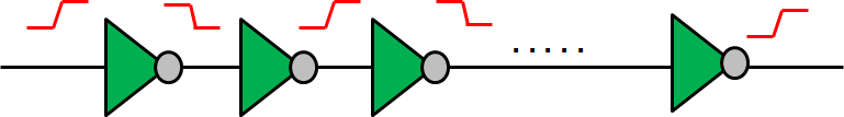
An inverter based clock tree:
To keep discussion simple, let us consider only one x kind of inverter to build our clock trees. And all the inverters are placed equidistant from each other. Advantage of using inverter based clock tree is that the high pulse and the low pulse width would be symmetrical. For the clock signal, this is a critical requirement, especially for SoC’s which have high interaction between positive and negative edge triggered flip flops.
A buffer based clock tree:
While theoretically, one can create a buffer sing two identical inverters connected back to back, that is generally not the way buffers are designed while designing the std cell libraries. To save area, the first inverter is typically of a lower drive strength and is placed very close to second inverter. The second inverter however is of higher drive strength.
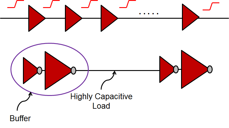
One must also notice that the delay of the first inverter is dominated by the load of the second inverter because the wire length between those two inverters is very small, hence one can neglect the wire cap. But for the second inverter, the load comprises of the wire cap as well as the input cap of the next buffer. This introduces an asymmetry in rise and fall delays, and hence is the high and low pulse widths of the clock signals.

For applications which have stringent requirement on clock high and low pulse widths, one might prefer to use an inverter based clock tree over the buffer based clock tree.
Can we do something to make the buffer based clock tree work ? YES!
If we balance the load seen by first inverter and load seen by second inverter, we might be able to achieve equal rise and fall times, and equal high and low pulse widths for clock transition signal.

To have equal pulse widths for high and low times, the RC delay observed by the first inverter must be equal to the RC delay of the second inverter.
Rchn1(Cd1 + Cg2) = Rchp2(Cd2+cg1+cwire) + Rwire/2(Cwire + Cg1) + Rwire/2(cg1)
A simple way to mitigate the problem is to insert an inverter in the middle point of the buffer based clock tree. The major challenge, however, lies in finding the middle point. This ensures that high and low pulse widths of the clock reaching at the sink points is indeed the same.
