
Low Power Design Strategies
Power consumption has become a very important factor in recent process nodes. In this article we will explore/discuss the increasing challenges of power consumption and various design strategies to reduce power consumption.
Increasing Challenges of power
In earlier generations of IC design technologies, the main parameters of concern were timing and area. EDA tools were designed to maximize the speed while minimizing area. Power consumption was a lesser concern. CMOS was considered a low-power technology with fairly low power consumption at the relatively low clock frequencies used at the time, and with negligible leakage current.
In recent years, however, device densities and clock frequencies have increased dramatically in CMOS devices, thereby increasing the power consumption dramatically. At the same time, supply voltages and transistor threshold voltages have been lowered, causing leakage current to become a significant problem.
High power consumption can result in high temperatures during operation. Higher operating temperatures also reduce reliability because of electromigration and other heat-related failure mechanisms.
Dynamic & Static Power
Dynamic power is consumed during the switching of transistors, so it depends on the clock frequency and switching activity. Static power is the transistor leakage current that flows whenever power is applied to the device, so it is not related to the clock frequency or switching activity.
Dynamic Power is the energy consumed during logic transition on the nets, consisting of two components switching and internal power. Switching power results from charging and discharging of external load cap on the output of the cell. Internal power results from short circuit current that flows through PMOS-NMOS stack during a transition.
Switching power - The amount of energy dissipated in each transition depends on the supply voltage and the capacitive load of the net. Also, because the current flows only during logic transitions on the net, the long-term dynamic power consumption depends on the clock frequency (possible transitions per second) and the switching activity.
Internal power - is consumed during the short period of time when both PMOS and NMOS are ON. This condition results in large current to flow from VDD to VSS (short circuit current - crowbar current). Lower threshold voltages and slower transitions result in more internal power consumption.
Static(leakage) Power Leakage current was negligible in earlier CMOS technology. But, with shrinking device geometries and reduced threshold voltages(scaling) leakage power is becoming significant enough that we cannot neglect it anymore.
Main causes for leakage power are
1) reverse bias p-n junction diode Leakage - has always existed in CMOS designs. This is the leakage from n type drain to p-type substrate in NMOS transistor and from p-type drain to n-type substrate in PMOS transistor.
2) sub-threshold leakage - is the flow of current from source to drain when the transistor is held “off”. However, with lower power supply voltages and lower threshold voltages, “off” gate voltages are getting close to “on” threshold voltages. Sub-threshold leakage current increases exponentially as the gate voltage approaches the threshold voltage.
In the past, the subthreshold conduction of transistors has usually been very small in the off state, as gate voltage could be significantly below threshold; but as voltages have been scaled down with transistor size, subthreshold conduction has become a bigger factor.
Subthreshold conduction or subthreshold leakage or subthreshold drain current is the current between the source and drain of a MOSFET when the transistor is in subthreshold region, or weak-inversion region, that is, for gate-to-source voltages below the threshold voltage.
The reason for a growing importance of subthreshold conduction is that the supply voltage has continually scaled down, both to reduce the dynamic power consumption of integrated circuits and to keep electric fields inside small devices low, to maintain device reliability.
The amount of subthreshold conduction is set by the threshold voltage, which sits between ground and the supply voltage, and so has to be reduced along with the supply voltage. That reduction means less gate voltage swing below threshold to turn the device off, and as subthreshold conduction varies exponentially with gate voltage
3) gate leakage - is the result of using an extremely thin insulating layer between the gate conductor and the MOS transistor channel. Gate oxides are becoming so thin that only a dozen or fewer layers of insulating atoms separate the gate from the source and drain. Under these conditions, quantum-effect tunneling of electrons through the gate oxide can occur, resulting in significant leakage from the gate to the source or drain.
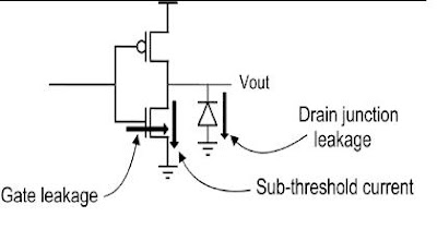
Leakage currents occure whenever power is applied to the transistor, irrespective of the clock speed or switching activity. Leakage cannot be reducde by slowing or stopping the clock. However, it can be reduced or eliminated by lowering the supply voltage or by switching off the power to the transistors entirely.


Including two other posts - GIVING BRIEF ; (https://eternallearning.github.io/power-reduction-methods-part1/) 3) (https://eternallearning.github.io/power-reduction-method-part2/)
Brief Rundown Why power matters now: Older nodes optimized mainly for timing/area since CMOS leakage was negligible. As device density and clock frequency scaled up and Vdd/Vt scaled down, both dynamic power and leakage grew dramatically — and high power → high temperature → reliability problems (EM, heat-related failures). Two power components:
Dynamic power — consumed during switching; depends on clock frequency and switching activity. Two sub-parts: Switching power — charging/discharging the external load cap on a cell’s output. Internal power — short-circuit (“crowbar”) current when PMOS and NMOS are momentarily both on during a transition; worse with lower Vt and slower slew. Static (leakage) power — flows whenever power is applied, independent of clock/switching. Three sources: Reverse-bias p-n junction leakage Sub-threshold leakage (current when transistor is nominally “off” — grows exponentially as Vt is scaled down with Vdd) Gate leakage (quantum tunneling through ultra-thin gate oxide) Leakage can’t be fixed by slowing/stopping the clock — only by lowering Vdd or cutting power entirely.
Fix Methods:
- Supply voltage reduction — fixes BOTH dynamic and static (leakage) power Dynamic power drops because switching power scales with Vdd² (CV²f relationship). Leakage also drops because sub-threshold leakage current is exponentially dependent on Vdd/Vt. This is why it’s the most powerful single lever — but the cost is symmetric too: lower Vt (needed to preserve speed at lower Vdd) actively worsens sub-threshold leakage even as the lower Vdd itself helps it, so the two effects partially fight each other. Net result depends on how much you drop Vt vs. Vdd.
- Clock gating — fixes dynamic power ONLY (switching power specifically) Stopping the clock prevents flops from toggling internally and driving their fanout, which eliminates switching power on that clock branch and downstream logic that would’ve been re-evaluated. It does nothing for leakage — the gated flop and its logic are still powered and still leak, just not switching. This is why clock gating alone can’t address a leakage-dominated design (typical at advanced nodes).
- Multi-Vt cells — fixes static (leakage) power, at a dynamic-power/speed cost Swapping to high-Vt where you have timing slack directly reduces sub-threshold leakage on those cells. It doesn’t touch switching power’s dependence on Vdd/load cap — it’s purely a leakage-vs-speed knob, not a dynamic power reduction technique. (Low-Vt cells stay where needed for speed, accepting their higher leakage as a localized cost.)
- Multi-voltage design (power domains) — fixes dynamic power primarily Running non-critical blocks at a lower Vdd domain directly cuts their switching power (CV²f). It has a secondary leakage benefit too since leakage also scales down with Vdd, but the design intent here is usually “give speed-insensitive blocks a lower Vdd to save dynamic power,” not a leakage-elimination technique — leakage still flows continuously in that domain since it’s still powered.
- Power switching / power gating — fixes BOTH, but specifically by eliminating them rather than reducing them This is the only technique that kills static (leakage) power outright — since the block has zero power applied, there’s no leakage path at all, not just a reduced one. It simultaneously eliminates all switching/internal power in that block since nothing is toggling. This is why the source calls out that it reduces “leakage power as well as switching power” — it’s the most complete fix, at the cost of the retention/isolation/controller overhead discussed earlier.