Placement of Clock Gating Cells
Should the clock gating cells be placed closer to clock source or closer to sink flops ?
Let us explore the pros and cons of two scenarios below:
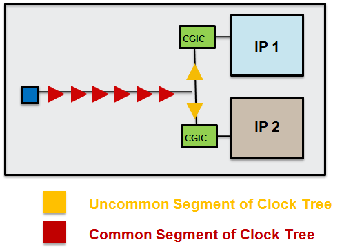
1) Clock Gating cells placed near the source: As shown in below figure, placing clock gating cells near source increase the uncommon path in clock structure. We know that we need to take OCV into effect because cells in uncommon path may behave differently for PVT variations. So, this extra uncertainty or pessimism needs to be taken into account while doing STA analysis. Such a scenario is hostile to timing convergence.
However, from power saving prospective this scenario is quite favorable. As soon as the clock gate is “off” all the clock buffers in the path are switched off. So, there is no toggling and dynamic power is reduced (switching power dissipation is not possible).

Also, another common problem with this kind of clock gate placement is, there might be setup violations seen at the enable pin of ICG. Figure below shows the scenario we are talking about. If ICG is more near to clock source then the capture clock latency is less than launch clock latency. Resulting in setup violation on clock enable pin of ICG.

2) Clock Gating cells placed near the sink: As shown in figure below, placing the clock gating cells near to sink flop reduces the uncommon clock paths making the timing easy to meet. But, the dynamic power is not saved. Because even if clock gate is enable all the clock buffers before that still toggle.
So, there is no one final answer for the clock gate placement. Depending on the design specs and requirements we can optimize for performance and/or power.
More notes on setup violation at clock enable pin - if ICG placed near to the source:
Ideally clock is balanced to the all sink pins( that is all flop clk pins). If we balanced to the clock pin of the ICG then the downstream registers driven by the ICG would have increased insertion delay relative to the rest of the registers in the design and as a result large skew. It would just be pushing the problem to other paths in the design.
Similarly, I think marking the output nets of the ICGs dont_touch isn’t suitable because it prevents the tool from optimizing in cases where buffering is required to reduce delay.
If I were looking at this design, I’d ask these questions:
What is the fanout of the ICGs in the cases where you’re seeing a setup violation on the enable pin? If it is greater than 32 or so I would think this is a case where you’d need to do cloning. If it’s less than 32 it seems like a case where the tool did a poor job placing the ICG at the center of gravity of the flops it drives.
Possible approaches to fix this: 1) If we are not seeing any violation on clk en pin in pre-cts but seeing violation in post-cts then we can make the tool see these en pin violations in PRE-CTS, that way maybe it will try to optimize the data path if possible.
2) Also, if fanout of the ICG is more than 32 flops, then cloning the ICG will help. If fanout is less than 32 but the design is still failing, then check if the icg aware placement is true or false and make sure to have it true in placement stage.
3) Create group path and add extra weight at placement for better optimization.